

Executive Overview
In the relentless race to sustain the computational demands of modern artificial intelligence, the global technology sector faces a looming physical and economic wall: power consumption. As machine learning models swell to trillions of parameters, the data centers powering them demand staggering amounts of electricity, pushing current silicon-based computer chip architecture to its absolute thermodynamic limits. For decades, semiconductor engineers have warned that conventional complementary metal-oxide-semiconductor (CMOS) scaling is reaching a bottleneck where further miniaturization generates unsustainable heat and energy loss.
Now, a team of materials scientists and engineers at Brown University has unlocked a breakthrough that could fundamentally rewrite the physics of microelectronics. Published in the prestigious journal Nature Materials, the research centers on a special class of materials known as multiferroics. These unique substances combine both electrical and magnetic properties that can be manipulated simultaneously using remarkably small voltages.
For years, the promise of multiferroics has tantalized physicists. Theoretically, they could enable computing architectures that operate on a fraction of the energy required by today’s processors. However, a stubborn physical barrier known as the "dead layer" effect has kept them out of commercial silicon chips. Whenever multiferroics are scaled down to the microscopic dimensions required for modern integrated circuits, they mysteriously shed the very electrical and magnetic properties that make them useful.
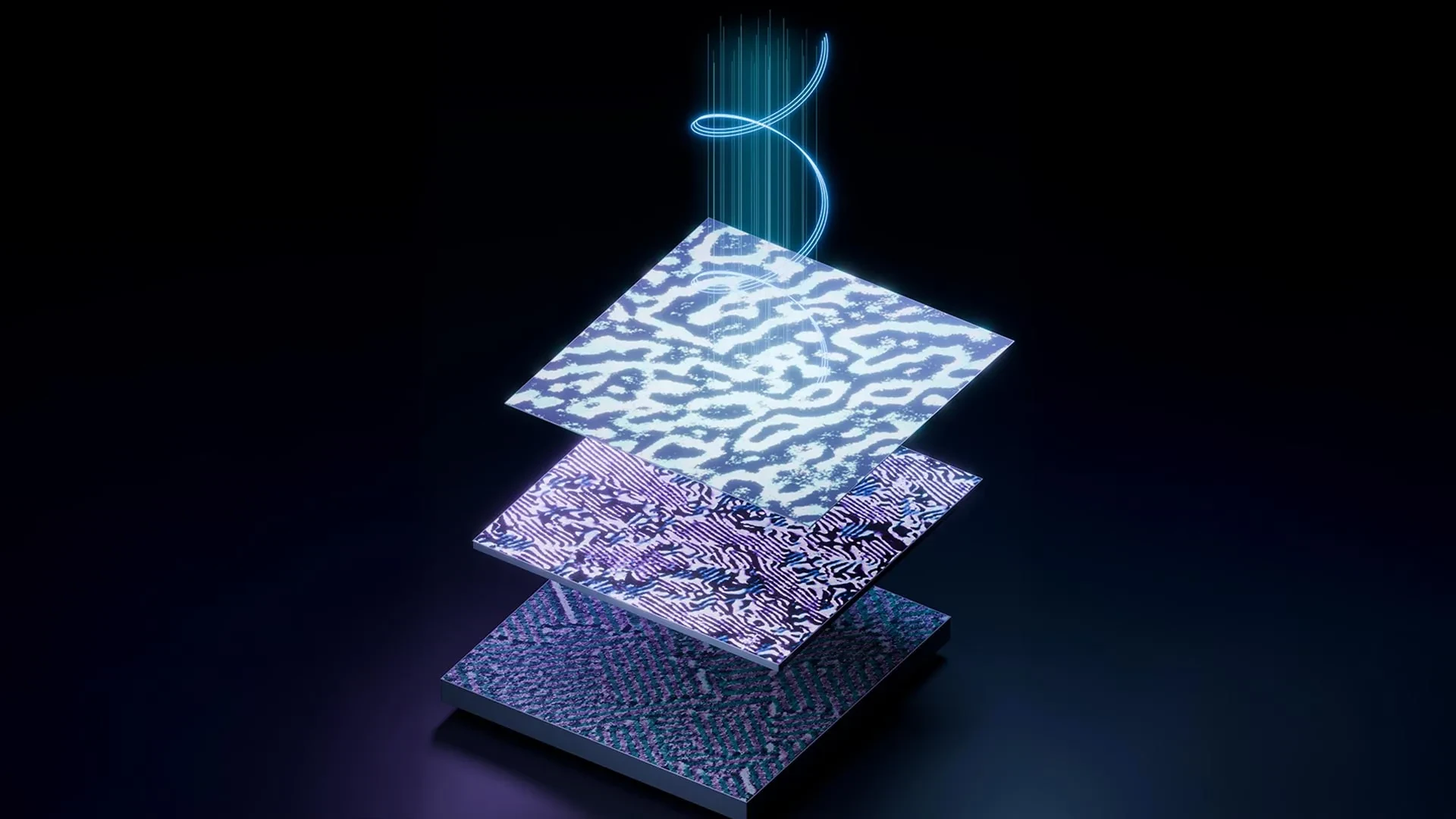
Led by Lucas Caretta, an assistant professor of engineering at Brown University, the research team has successfully vanquished the dead layer effect. By engineering the atomic environment of a premier multiferroic material—bismuth ferrite—the team produced ultra-thin films that retain their vital ferroelectric and magnetic characteristics down to a few angstroms. Even more astonishingly, the fabrication process unlocked an exotic, highly desirable form of magnetism known as altermagnetism. This development bridges the speed of antiferromagnets with the read-out ease of ferromagnets, offering a transformative blueprint for the next generation of energy-efficient AI hardware.
Detailed Chronology and Scientific Breakthrough
To understand the magnitude of the Brown University team’s achievement, one must trace the timeline of the roadblock that has frustrated condensed-matter physicists for over a generation.
The Anatomy of the Dead Layer
Multiferroics—and bismuth ferrite in particular—are prized because of their internal atomic architecture. They feature repeating crystal units where positive and negative electrical charges are permanently separated on opposite sides, creating a persistent electrical polarization. By applying a minute external voltage, engineers can flip this polarization, effectively rewriting the binary ones and zeros of digital information using almost negligible amounts of electrical current. Furthermore, because the material’s magnetic orientation is intrinsically coupled to its electrical polarization, stored data can be read magnetically.
The theoretical elegance of this mechanism is undeniable. Yet, translating bulk multiferroics into the nanoscale dimensions of modern microprocessors triggered a devastating material failure:
- Structural Distortion: When sliced into ultra-thin films to fit inside computer chips, the atomic lattice of the multiferroic undergoes mechanical strain from the underlying substrate, fracturing the delicate chemical environment necessary for polarization.
- Internal Electric Fields: Depolarizing fields naturally build up within thin-film geometries, aggressively counteracting the material’s internal electrical polarization until it collapses entirely.
Together, these forces create a non-functional boundary zone—the dead layer—rendering nanoscale multiferroics electrically and magnetically inert.
The Brown University Intervention
To bypass this historical hurdle, Caretta and his colleagues developed a sophisticated, two-pronged deposition technique designed to force bismuth ferrite to maintain its structural integrity at atomic scales.
First, the researchers selected a specialized foundational substrate made of dysprosium scandate, a rare-earth-derived compound. The crystal lattice of dysprosium scandate possesses dimensions slightly smaller than those of bismuth ferrite. When the bismuth ferrite is deposited onto this foundation, the lattice mismatch forces the multiferroic film under intense, uniform compressive strain. This physical squeeze acts like an atomic scaffolding, stabilizing the crystal structure and preventing the structural distortion that typically destroys ferroelectricity.
Second, to neutralize the internal electric fields that historically sabotage thin-film polarization, the team integrated a secondary metallic capping layer. This layer acts as a localized electrostatic shield, actively counteracting the unwanted fields and preserving the material’s internal charge separation.
When deployed in tandem, these engineering interventions completely eliminated the dead layer. The bismuth ferrite film successfully retained its ferroelectric and magnetic behavior even when compressed to a thickness of merely a few angstroms.
The Accidental Discovery of Altermagnetism
While proving that the dead layer could be conquered was a landmark achievement in its own right, the research yielded an unexpected scientific bonus. The engineered stress and structural alignment imposed by the substrate and capping layers did not merely preserve bismuth ferrite’s native properties—it actively transformed them.
The resulting ultra-thin films began exhibiting altermagnetism, a newly categorized magnetic phase that bridges the gap between traditional ferromagnetism and antiferromagnetism.
- Ferromagnets feature atomic magnetic moments that all point in the same direction, generating strong magnetic signals that are easily read out. However, they are notoriously sluggish in switching states and produce large stray magnetic fields, making it difficult to pack them densely onto a microchip without cross-talk interference.
- Antiferromagnets feature neighboring magnetic moments pointing in opposite directions, canceling each other out. This allows them to switch at blistering speeds and generate zero stray magnetic fields, but their canceled fields make reading data extraordinarily difficult.
- Altermagnets combine the best of both paradigms. They offer the lightning-fast switching speeds and stray-field immunity of antiferromagnets, while retaining strong, direction-dependent electrical signatures that allow engineers to read data easily.
By forcing bismuth ferrite into an altermagnetic state at nanometer scales, the Brown team opened a direct pathway toward high-density, ultra-fast, low-power memory and logic components.
Supporting Context and Metrics: The Energy Crisis in Computing
The urgency of breakthroughs like Caretta’s cannot be overstated. The digital infrastructure underpinning the modern global economy is hurtling toward an energy wall driven primarily by the exponential scaling of artificial intelligence.
The AI Power Crunch
Modern Large Language Models (LLMs) require training runs that consume megawatt-scale power installations, frequently rivaling the electricity consumption of small towns. As these models scale from billions to trillions of parameters, hardware architectures are pushed to their absolute physical limits.
Standard silicon chips rely on field-effect transistors (FETs) that require a constant flow of electrical current (and the resulting generation of Joule heat) to switch bits. In a conventional processor, billions of transistors switch billions of times per second, generating immense thermal loads that demand aggressive, power-hungry cooling systems.
The Multiferroic Efficiency Advantage
Multiferroic devices operate on fundamentally different physics. Because switching is controlled primarily via voltage-driven polarization rather than continuous current flow, the energy required to change a bit of data drops by orders of magnitude.
| Metric / Feature | Conventional Silicon CMOS | Multiferroic (Bismuth Ferrite) Approach |
|---|---|---|
| Primary Switching Mechanism | Current-driven electron flow (Charge) | Voltage-driven polarization coupling |
| Energy Consumption per Switch | Relatively high (Joule heating losses) | Ultra-low (Minimal static current) |
| Integration Density | Constrained by thermal dissipation and stray magnetic fields | High density enabled by stray-field-free altermagnetism |
| Operating Speed | Moderate to High (Thermal bottlenecks) | Extremely High (Altermagnetic dynamics) |
By integrating altermagnetic bismuth ferrite into microchips, engineers could theoretically construct non-volatile memory and logic gates that consume negligible static power and generate virtually zero waste heat, fundamentally altering the economics and environmental footprint of AI infrastructure.
Official Statements and Academic Insights
The implications of the study have resonated deeply across the materials science community, signaling a shift from passive observation of material physics to active, bottom-up quantum engineering.
"We’ve established that we can get rid of the dead layer," said Lucas Caretta, assistant professor of engineering at Brown University and principal investigator of the study. "We show that you can make this material basically as thin as you want—down to a few angstroms—and it’s still ferroelectric, and it’s still magnetic."
Caretta emphasized that the discovery highlights a paradigm shift in how scientists approach advanced materials. Rather than hunting endlessly through nature for a compound that naturally possesses every ideal engineering trait at the nanoscale, modern fabrication techniques allow scientists to coax exotic, superior behaviors out of known bulk materials.
Elaborating on the unique advantages of the newly unlocked magnetic phase, Caretta explained the operational bottleneck facing conventional microchip design:
"Ferromagnets are useful for memory and logic because they produce strong magnetic signals that are easy to read out. The challenge is that they are relatively slow, and their stray magnetic fields make it difficult to pack devices densely on a chip without interference. Antiferromagnets can operate much faster and avoid those stray fields, but their signals are much harder to detect. Altermagnets are kind of the best of both worlds—they can be fast, densely integrated and still provide a strong electrical signal for readout."
This multidisciplinary effort was made possible through competitive, peer-reviewed backing from major federal science agencies. The research team received foundational funding support from the U.S. Army Research Office (Grant W911NF-21-2-0162), the National Science Foundation (Grants DMR-2039380 and OIA-2327352), and the U.S. Department of Energy (Grant DE-AC02-05CH11231), underscoring the critical national security and economic importance of next-generation microelectronics.
Future Outlook: The Road from Lab to Fab
While the publication in Nature Materials marks a monumental scientific milestone, the transition from an academic laboratory breakthrough to a commercial semiconductor fabrication line ("fab") involves significant hurdles.
Scaling and Manufacturing Integration
Semiconductor manufacturing is arguably the most complex and precise industrial process on Earth, anchored entirely to silicon wafer processing infrastructure. Integrating novel oxide materials like bismuth ferrite—often referred to in the industry as "ferroelectric oxides"—into standard complementary metal-oxide-semiconductor (CMOS) manufacturing lines requires developing new deposition protocols.
Foundries must learn to deposit ultra-thin epitaxial films of bismuth ferrite uniformly across 300-millimeter silicon wafers without contaminating traditional manufacturing tools with incompatible elements like bismuth, iron, or rare-earth scandates.
Next Steps for the Brown Team
Caretta and his collaborators are already turning their attention toward these scaling challenges. Their immediate roadmap involves:
- Wafer-Level Integration: Testing the deposition of strain-engineered bismuth ferrite on silicon-compatible substrates to prove compatibility with industrial semiconductor tools.
- Prototype Logic and Memory Cells: Designing functional prototype transistors and memory storage cells utilizing altermagnetic bismuth ferrite switching elements to quantify real-world energy savings.
- Dynamic Testing: Measuring switching speeds and endurance cycles under high-frequency operational loads to ensure the material can withstand the billions of cycles required by commercial microprocessors.
A Transformative Horizon for AI
As artificial intelligence models scale toward artificial general intelligence (AGI), the hardware bottleneck will only intensify. Solutions that rely purely on incremental tweaks to silicon geometry are nearing a dead end.
The work conducted at Brown University demonstrates that the periodic table holds vast, untapped potential if approached with creative atomic-level engineering. By shattering the dead layer effect and unlocking altermagnetism in ultra-thin multiferroics, Caretta and his team have sketched the blueprints for a cooler, faster, and infinitely more energy-efficient computational future.
As Caretta concluded, summarizing the philosophy driving modern materials science:
"We know the underlying properties are already there in the bulk materials. The trick is learning how to engineer them into a form that’s useful—and sometimes even better than what nature gives us."
